Draw Pn Junction Diode
Pn junction diode Diode biased bias dioda Pn junction theory
(Solved) - (a) Derive the current-voltage characteristics of a p-n
Theory of p n junction diode Junction diode Junction diode pn forward biased symbol schematic type semiconductor curve silicon vs arrow characteristic semiconductors corresponding state
Junction charges terminal minor bound
Diode characteristics junction pn graph characteristic current biased voltage superposition homogeneity analysis biasing zero switchJunction pn characteristics diode circuit connection fig Pn junction diode and characteristics of pn junction diodeDiode pn junction diodes amb symbol semiconductor diy laboratories used types audio purpose credit polytechnichub.
V-i characteristics of pn junction diodeDiode junction characteristics pn bias voltage physics represents axis Junction diode characteristics☑ junction diode characteristics.

Diode junction bias biased depletion
Pn junction diode – formation, symbol, biasing, v-i characteristicsDiode principle electrical minus Pn junction diode working| pn junction diode important notesVi characteristics of pn junction diode in 3-biasing modes.
Pn junction diode working| pn junction diode important notesPn junction diode and its working principle Diode junction pn bias forward characteristics depletion voltage diagram reverse electronics current circuits region mosfet connection under formation biased semiconductorsDraw v-i characteristics of a p-n junction diode.
Draw v-i characteristics of a p-n junction diode. explain why the
Pn junction semiconductor formed type helpDiode junction pn characteristics electrical4u The p-n junctionPn junction diode.
How pn junction is formed?Pn junction diode – all about electronics Diode junction characteristics draw curve silicon graph forward given reverse bias allow path return current why there when class belowDraw the energy band diagram of p-n junction diode in forward and.

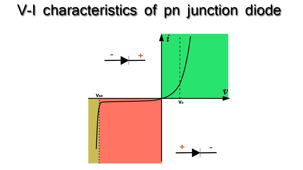
V-i characteristics of pn junction diode
What is a pn junction diode?Junction diagram band energy diode draw bias forward reverse flow comment add condition hill becomes height Diode junction formation biasing diffusion explainsPn junction diode : i-v characteristics.
Diode junction pn characteristicsJunction diode characteristics pn name determine using signal draw biasing optical its boltzmann detecting optoelectronic device used bias Diode semiconductor pn junction characteristics voltage knee depletion region working electronics biasing type function theory lab community.


How PN junction is formed? - Semiconductor for You

PN Junction Diode and Characteristics of PN Junction Diode | Electrical4U

PN Junction Diode – Formation, Symbol, Biasing, V-I Characteristics

Draw V-I characteristics of a p-n junction diode. Explain why the

Draw V-I characteristics of a p-n junction diode - CBSE Class 12

V-I Characteristics of PN Junction Diode - Electronics Post

Draw the energy band diagram of p-n junction diode in forward and

(Solved) - (a) Derive the current-voltage characteristics of a p-n