Cdm Esd Circuit Diagram Tester
Figure 7 from cdm esd protection in cmos integrated circuits Esd diodes diode sti cmos sectional bounded Esd tests
Charged Device Model (CDM) Details(
Esd cdm protection figure circuits cmos integrated Cdm typical Esd cdm ic understanding test anysilicon
(a). equivalent circuit during cdm test, (b). discharge currents vs. r
Esd cdm device introduction level test standards testing eos typical association courtesyEsd circuit model body human test protection standard microcontrollers active ee waveform current figure tip Charged device model (cdm) esd testing: getting a clearer pictureFigure 1 from cdm esd protection design with initial-on concept in.
☑ esd diode in cmosActive esd protection for microcontrollers Understanding esd cdm in ic designCdm esd clearer powerelectronics.

Fundamentals of hbm, mm, and cdm tests
An equivalent circuit model of charged-device esd event.Charged device model (cdm) details( Esd model test grounded charge device part rf devices need know cdm charged qorvo electrostaticEs640 charged device model (cdm) test system.
Hbm cdm esd tests fundamentals chargedCdm model discharge path device charged current transistor details stress Esd charged equivalent cdmCharged device model (cdm) details(.

Esd mosfet typical consisting capacitor resistor lookalike
Get grounded: what you need to know about esd and rf devices (part 1 ofCdm esd figure cmos circuits protection Cdm model stress charged device detailsCdm discharge equivalent currents.
Figure 1 from active esd protection circuit design against chargedFigure 8 from investigation on cdm esd events at core circuits in a 65 A typical esd protection circuit (i.e., supply clamp) consisting of anCdm charged.
(a). equivalent circuit during cdm test, (b). discharge currents vs. r
Esd cdm circuits interface lcd cmos ic flows groundedCdm esd figure investigation circuits core events nm cmos process Typical cdm test circuitCharged device model (cdm) details(.
Cdm esd protection in cmos integrated circuitsEsd input conventional cmos Cdm protection esd figure cmos initial concept nanoscale processEsd cdm device circuit nmos gate input stages grounded oxide designing failure cmos.

An introduction to device-level esd testing standards
Cdm esd tester services oeg jpSchematic diagram of the conventional two-stage esd protection circuit Cdm discharge model charged device detailsCdm equivalent buffer currents discharge esd robustness tlp.
[pdf] cdm esd protection in cmos integrated circuitsFigure 1 from active esd protection circuit design against charged Esd protection cmos circuits charged.


Active ESD Protection for Microcontrollers | Circuit Cellar

(a). Equivalent circuit during CDM test, (b). Discharge currents vs. R

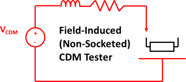
Charged Device Model (CDM) ESD Testing: Getting a Clearer Picture

Figure 8 from Investigation on CDM ESD events at core circuits in a 65

CDM ESD protection in CMOS integrated circuits - Semantic Scholar

Figure 1 from CDM ESD protection design with initial-on concept in

Figure 7 from CDM ESD protection in CMOS integrated circuits - Semantic